Observation and Measurement of Ball Grid Arrays (BGA) Using a Digital Microscope
The spread of 5th generation mobile communication systems (5G) has led to semiconductor devices becoming smaller and more integrated, and has also increased demand for product inspection and analysis.
This section introduces examples of observation and measurement of the bumps of BGAs, which are common observation targets for digital microscopes.
- Typical IC Packages
- Typical Bonding for IC Chip Mounting
- Bump Making Methods for Flip-chip Bonding
- Examples of Observation and Measurement of BGAs (Bumps) Using a Digital Microscope
Typical IC Packages
As ICs become more integrated ICs, surface mount technology (SMT) has become mainstream. Matrix type (BGA type) packages are used for highly integrated ICs.
This section introduces the following typical IC packages.
Surface mount technology (SMT): Non-lead type package
- SON (small outline no-leaded) package
-
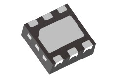
These are SMT packages with no leads. Electrode pads are used as connection terminals. SON are two-way type packages used for small numbers of pins.
- QFN (quad flat no-leaded) package
-
These are SMT packages with no leads. Electrode pads are used as connection terminals. QFN are four-way type packages.
Surface mount technology (SMT): Matrix type package
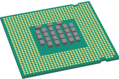
- BGA (ball grid array)
-
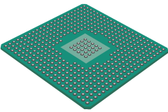
Solder balls (sphere shaped) are arrayed on the bottom of the package to use as terminals.
- PGA (pin grid array)
-
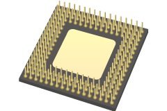
Pins are arrayed on the bottom of the package to use as terminals.
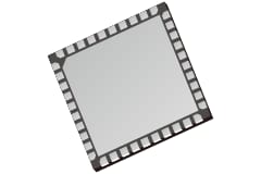
- LGA (land grid array)
-
Electrode pads (incl. copper pads) are arrayed on the bottom of the package to use as terminals.
Typical Bonding for IC Chip Mounting
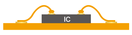
- Wire bonding
-
Wire bonding is used to connect semiconductor chip electrodes to the electric conductors of lead frames or boards with thin wires of gold, aluminium, or copper.
- Flip-chip bonding
-
The method where IC chips are attached directly to a PCB is called FC-BGA (Flip Chip-BGA). Bumps are made on the electrodes of an IC chip and then connected to the electrodes of a PCB. This saves space, compared to wire bonding.
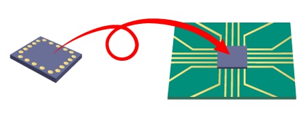
- Left: IC chip
- Right: Flip (face down)
Bump Making Methods for Flip-chip Bonding
- Solder ball mounting
- Solder balls are made in advance, placed on the electrodes, and then reflowed to make bumps. Higher bumps can be made than is possible with paste printing. Unifying the size of solder balls also prevents bump height differences.
- Paste printing
- Solder paste is printed on the electrodes, and then reflowed to make bumps. Throughput is high, but it is difficult to unify the bump height.
- Plating
- Electroplating is used to make solder bumps. Fine bumps can be made, but throughput is low.
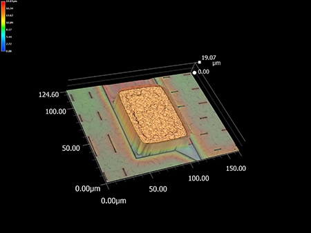
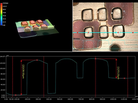
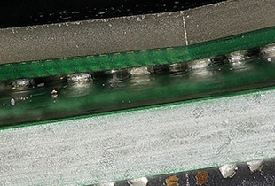
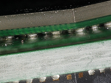
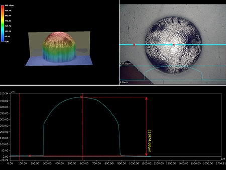
Examples of Observation and Measurement of BGAs (Bumps) Using a Digital Microscope
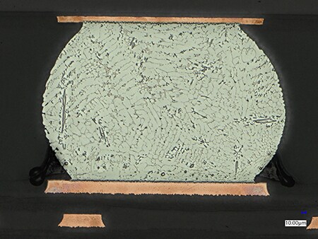
The latest examples of observation and measurement images of BGAs (bumps) using KEYENCE’s VHX Series 4K Digital Microscope are introduced below.
100×, ring illumination
Tilted observation allows observation of BGA balls through a clearance on a PCB.
300×, mixed illumination (glare removal image)
Mixed illumination and the glare removal function allow for observation without glare.