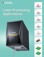
Laser Marking Systems / Laser Markers
Laser Marking in the Semiconductor Industry
Direct Part Marking in the Semiconductor Industry
Semiconductor laser marking is a process that uses a laser marking system to mark semiconductor devices with identifying numbers, barcodes, or logos. The laser marking system directs a beam of high-energy light at the semiconductor device, which heats the surface of the device and causes it to change colour. This change in colour is used to create the markings that can provide part branding or traceability.
Semiconductor laser marking is an important part of the semiconductor manufacturing process, as it allows for the easy identification of semiconductor devices. In addition, semiconductor laser marking can be used for other purposes, such as part marking and barcoding.
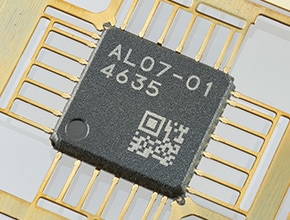
IC packages
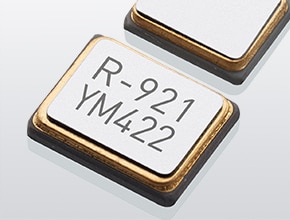
Crystal oscillators
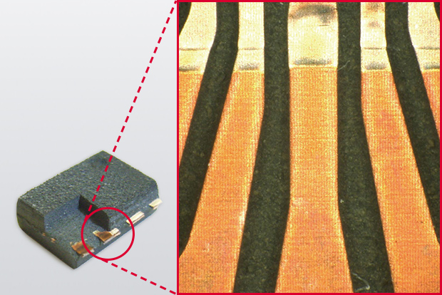
Wafers

Moulded packages
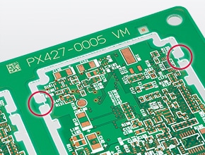
Glass epoxy PCB

Wire sheath
Epoxy package
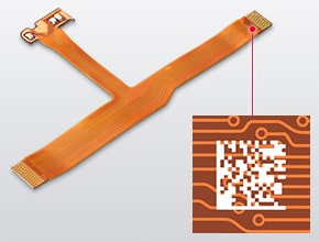
Flexible PCB
Semiconductor manufacturing is the process used to create semiconductor devices, which are electronic components made from semiconductor materials. These materials are typically silicon-based, but can also be made from other materials such as germanium, gallium arsenide, or silicon-germanium. The parts are commonly used in computers, hand-held electronic devices such as mobile phones, tablets and electronic book readers, wearable devices and consumer electronics.
This manufacturing process starts with wafer fabrication, in which these materials are purified and shaped into thin disks called wafers. These wafers are then subjected to a series of complex processes that add electrical components such as transistors and other circuit elements. Also, many parts require laser marking before they are packaged and shipped to the customer.
Semiconductor manufacturing is a highly complex and precise process, and even small changes in the fabrication process can significantly impact the finished product's performance. That said, using precise and professional equipment is paramount, including the right semiconductor laser marking systems.
These laser marking machines are used to create semiconductor devices such as semiconductor chips, wafers, printed circuit boards (PCBs), integrated circuits (ICs), and other semiconductor devices.
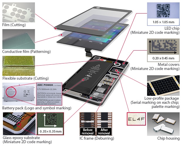
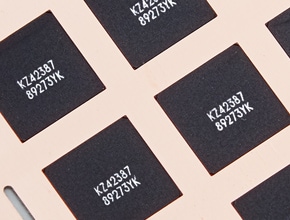
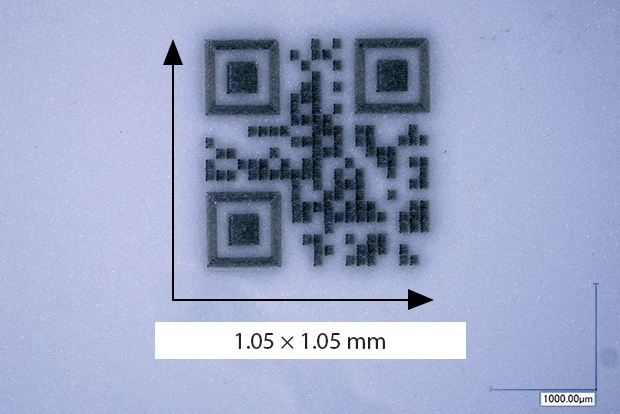
Micro and 2D Code marking on IC Chips
Until recently, IC chips were only marked with lot codes. However, a growing need for encoded data has prompted many manufacturers to start using 2D codes.
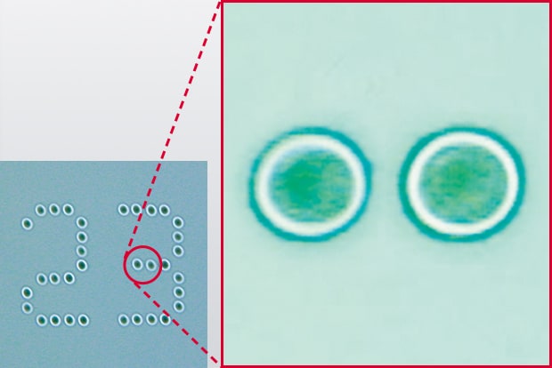
Micromarking
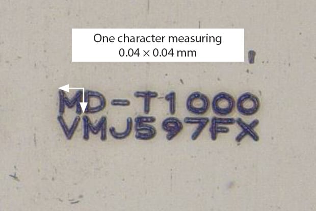
Laser markers have a very small beam spot, making them perfect for applications with a limited marking area. Micromarking - which is typically impossible for most systems - can be accomplished with the right laser. Various marking styles can also be selected, from shallow marking to deep engraving.
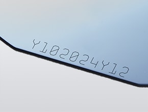
Marking silicon wafer
It's vital to keep surface damage to a minimum when marking a finished wafer, otherwise dust and debris can form. That's why UV and green lasers are the optimal wavelengths for these applications
Marking LED ceramic package
Due to space limitations, ceramic packages often use 2D codes to contain all the necessary traceability information.
Plating and Coating IC Chip Removal
KEYENCE’s 3-Axis laser markers can mark the top surface of IC chips and remove plating or coatings within the same process. Since the laser accurately scans only along the edges of the IC, flash burrs over the leads can be removed without causing damage to the inside of the package.
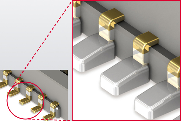
Removal of gold plating on terminals
To prevent solder wicking, lasers are used to remove the gold plating from connector terminals.
In the past, masks were used to avoid unnecessary plating. Today, connectors are designed smaller and thinner, and the pitches between the terminals are narrower. Consequently, it has become common practice to apply plating and then remove it with a laser for micron accuracy.
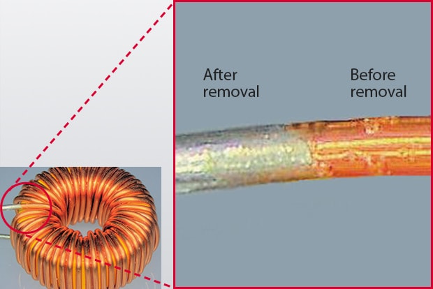
Removal thin-film coil coating
Previously, removers or edged tools were generally used to remove thin-film coating from coils. Now, laser markers have become useful because they require no consumables and ensure stable results.
Resin coating removal
Chemicals are often used to remove resins on defective moulds so that the moulds can be analysed. However, chemicals can damage the internal circuit and require multiple man-hours of work. Using a laser marker to remove resin saves running costs and time.
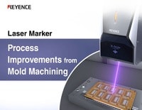
Benefits of Laser Marking Semiconductor Parts
In the semiconductor industry, semiconductor laser marking is used extensively for part marking. This is because semiconductor laser marking machines offer many advantages over other types of machines. For example, semiconductor laser marking machines can mark very small parts with a high degree of accuracy. In addition, semiconductor laser marking machines are very fast, so they can mark large quantities of parts in a short period of time.
The process is also highly versatile, allowing for a wide range of semiconductor part designs and markings. Additionally, semiconductor laser marking is an environmentally friendly alternative to other part marking processes, such as etching or screen printing, because it does not use any consumables. As a result, semiconductor laser marking machines are an essential part of the semiconductor industry.
KEYENCE - The Right Laser Marking Partner for the Semiconductor Industry
KEYENCE manufactures and develops custom laser marking systems for the semiconductor industry. We serve as an extension of your team to help you improve and automate your factory. Additionally, our knowledgeable team and trained sales force can help solve challenging and technical problems related to semiconductor part marking.
Ready to improve your semiconductor-related processes? Contact us today or view our laser marking systems to learn how we can help.
Application Video
FAQs about Laser Marking in the Semiconductor Industry
What types of lasers are used in wafer manufacturing?
Two of the most common types of lasers used in wafer manufacturing are near infrared and UV lasers. Historically, near infrared lasers have been the industry standard, but new developments in UV systems have shifted the needle in their favour.
Why do semiconductor wafers need to be laser marked?
Traceability is the driving factor behind laser marking in this industry. Semiconductors go through many steps prior to distribution, so it is important to have 100% traceability to ensure each procedure has been met and faulty products are separated before reaching the customer.
What are challenges of laser marking in the semiconductor industry?
As advancements grow the size of components shrink for this industry. This level of intricacy highlights the need for premium beam control and limited heat affected zones. In addition to increasing demand for precision the general application scope tends towards a more technical need. Keyence stands alone in providing local product specialists to work with your team to see how lasers could benefit your process.
How are lasers used in semiconductor manufacturing?
Historically, lasers have been used to mark content for traceability or branding purposes. Recent advancements have opened the door to a new realm of applications when it comes to laser processing. The same lasers used for traceability have the capability to precisely alter surface properties or remove material making lasers a versatile tool for semiconductor manufacturers.
![Laser Marker Installation Examples [Electronic Device Industry]](/img/asset/AS_117224_L.jpg)